
How can structures smaller than one micrometer be generated? And how can even smaller structures of less than 100 nanometers be produced without great effort? Scientists at the Fraunhofer Institute for Laser Technology ILT have developed several technologies to simulate, produce and measure periodic microstructures. They use phase-shifting transmission masks that can efficiently generate nanostructures down to 28 nanometers.
By Fraunhofer Institute for Laser Technology
For over 50 years, the density of transistors on integrated circuits has doubled approximately every two years. Adhering to this law, formulated by Gordon Moore, is made possible by ever new advances in microlithography. The technical progress behind it is immense. However, in the meantime, the system technology required to produce the smallest structures has also become immense. A microlithography system of the latest generation costs well over 100 million dollars and weighs 180 tons.
Dr. Serhiy Danylyuk, team leader of EUV and DUV Technology at Fraunhofer ILT in Aachen, describes the strategy of his working group.
“To counter this trend, we are developing technologies for the production of nanostructures that start-ups or medium-sized companies can also afford.”
Sub-Micrometer Structuring of Surfaces With Deep-UV Lasers
The basic idea is to generate periodic structures via the interference effects of coherent radiation, like the achromatic Talbot effect. In the near field, i.e. less than 500 µm behind a mask, an intensity distribution is created with which microlithographic structures can be produced.
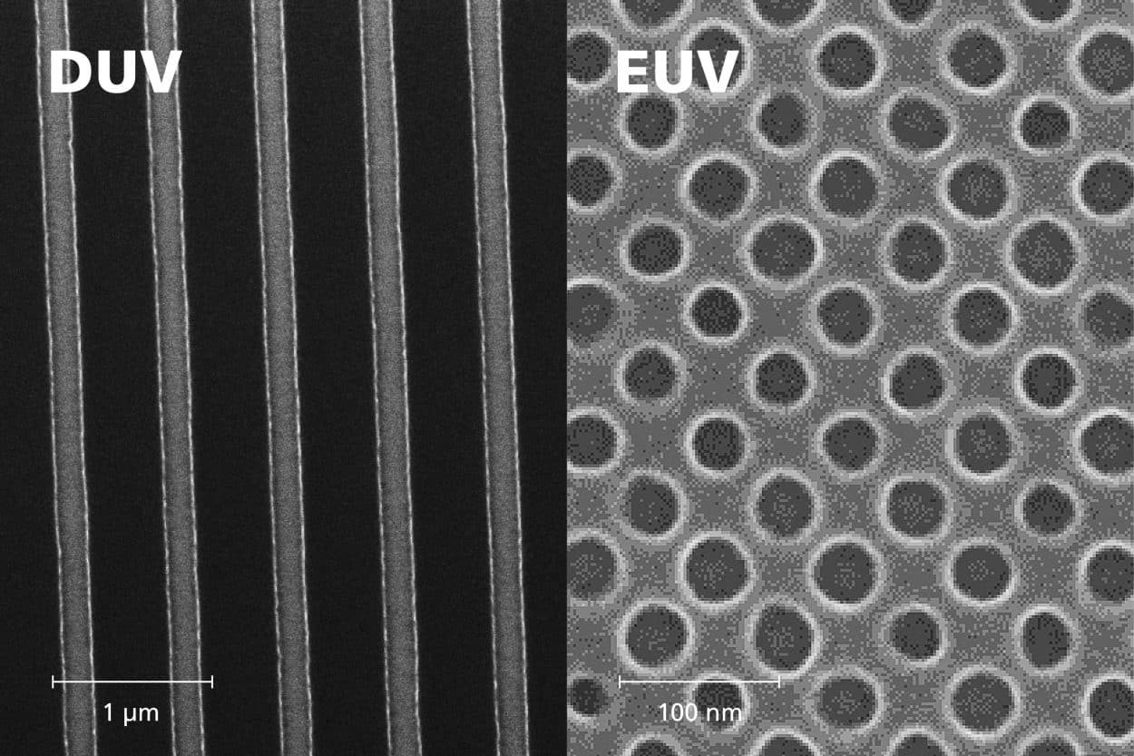
Using a KrF excimer laser at a wavelength of 248 nm, scientists at Fraunhofer ILT can generate structures with a period of several hundred nanometers. They have tested this with a LEAP150K laser system from Coherent, installed in the Excimer Lab of the institute. In a photoresist, 180 nm wide lines can be generated with a period of 600 nm. With higher energies of 250 mJ/cm², silicon on glass can also be ablated with similar dimensions. Furthermore, this technology is well suited for the ablation of PET plastic surfaces on a 300 nm scale.
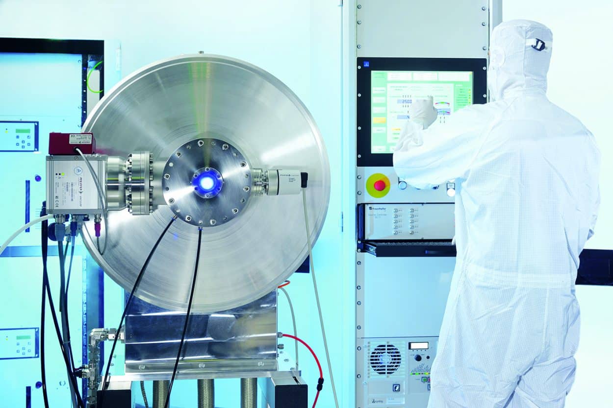
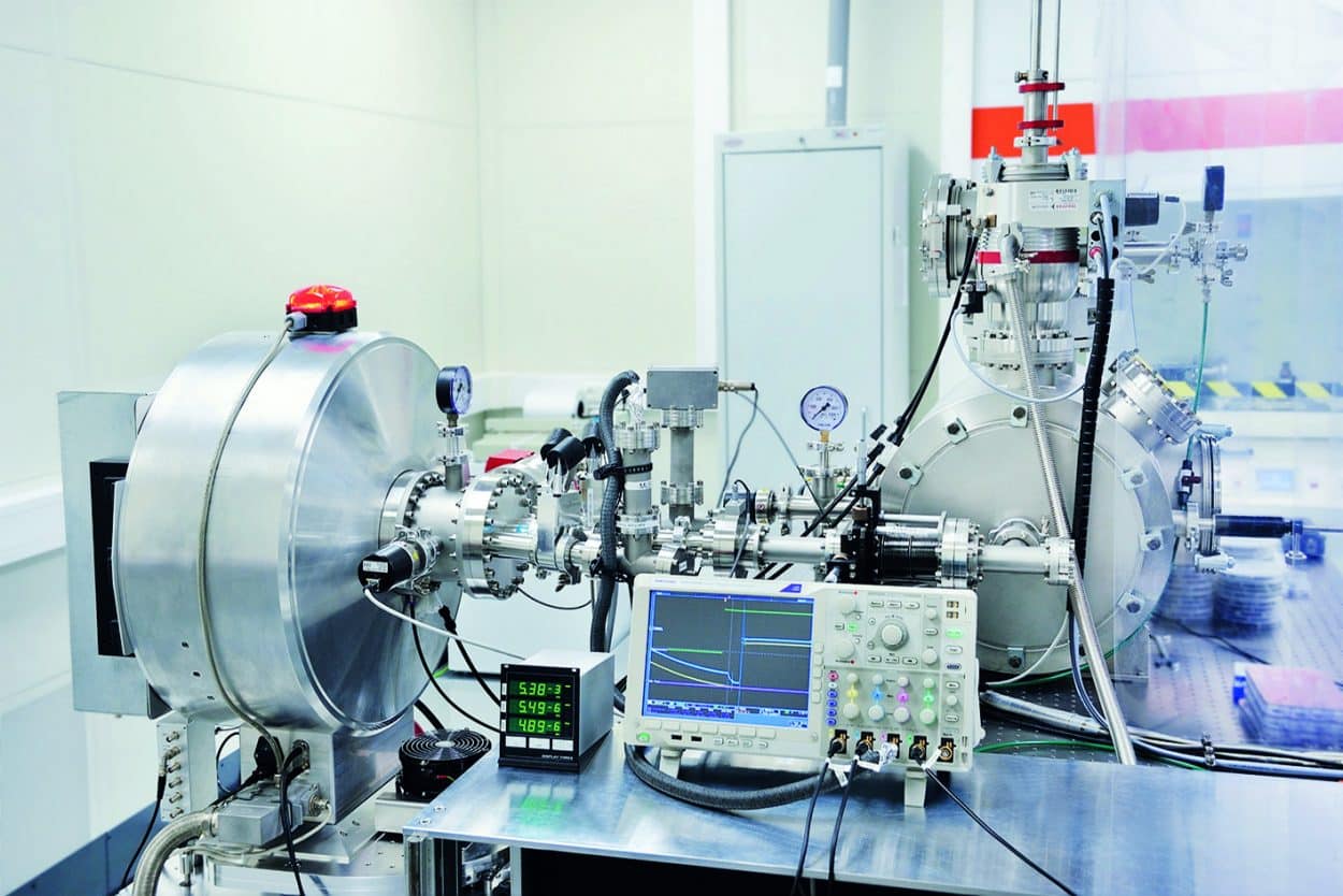
Discharge-Based EUV Source for Structures Smaller Than 100 NM
The principle also works with wavelengths in the extreme ultraviolet (EUV). The Aachen-based institute has developed its own beam source for this purpose, the “FS5440”. Based on a gas discharge, the source can generate the required radiation at 13.5 nm wavelength. It is considerably more compact than the laser-based EUV source used in large-scale industrial facilities. Nevertheless, the performance is more than sufficient for many applications in the production or measurement of nanostructures.
The EUV source is equipped with power and spectrum monitoring and generates up to 40 W at 13.5 nm in +/-1 percent bandwidth. The available intensity in the mask plane is more than 0.1 mW/cm². Thus, wafers with a diameter of up to 100 mm can be processed in Fraunhofer ILT’s facility. In the test, structures with a size of 28 nm (half pitch) were produced using the achromatic Talbot effect. This is a world record for a compact EUV system. In the future, the resolution is to be increased even further down to 10 nm.
Focusing on Medium-Sized Businesses
Periodic nanostructures have various applications. For example, they are ideal for testing new resists in the EUV range. The technology developed at Fraunhofer ILT also makes it possible to create complex geometries and structures, using computer-aided lithography methods. For example, nanostructured coatings can be built on broadband reflecting mirrors for high-power lasers or nano-antennas for special plasmonic structures
The experts at Fraunhofer ILT aim to achieve sustainable technology development, project manager Danylyuk explained:
“It is important for us to be able to offer the complete process chain. That’s why we have established many required processes in-house, including optical simulations, mask production and the quality and composition measurements of surfaces and thin layers.”
That way, start-ups or interested medium-sized companies can be provided with access to this cutting-edge technology at reasonable investment costs. Further details will be presented at the online conference SPIE Photomask Technologies + EUV Lithography from September 21 to 25.